 CORPORATE OVERVIEW CORPORATE OVERVIEW
Founded in 1999 and based in Santa Clara, California, POLYSTAK provides silicon�based multi chip package products as well as package stacking solutions and repair services on both components and module level for customers in the wireless communications and computer/networking industries.
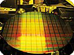
Started as a memory module company, POLYSTAK designed DRAM memory modules and developed memory module testers that has been supplied to the world's leading semiconductor. POLYSTAK also developed TSOP package stacking solution and has provided quality proven stacked DRAM packages to the one of world's largest semiconductor as well as many leading memory module makers.
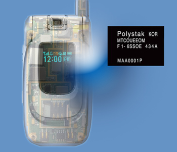
Based on the experience gained from memory stacking business, POLYSTAK started to offer Flash memory base MCP products for mobile handset industry and provide rework/repair services on both memory module and component level for computer/networking customers.
POLYSTAK recently reorganized and redistributed its resources to become a company that specialized in customized Multi Chip Packaging solution which plays critical role in compact but sophisticate and multi functional electronic devices such as mobile phones where its limited space restricts the freedom of design while the variety of function requires different combinations of integrated circuits.
Currently POLYSTAK provides multi chip package products to world's leading mobile phone manufacturers in Korea and is actively seeking opportunities to serve wireless customers in other continents.
|


 Copyright 2009, POLYSTAK, Inc. All rights reserved. Privacy Policy and Terms & Conditions