3D Memory Stacking
|
|
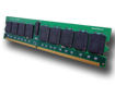
By stacking two or more memory chips, POLYSTAK effectively produces single memory components with significant advantages over single-chip devices of comparable density. The three of most prominent advantages are:
|
 |
 availability in high volume before the same-density, single-chip solution comes to market availability in high volume before the same-density, single-chip solution comes to market
cost effectiveness until the same-density monolithic device drops to price parity
significant space saving via 3D structure |
|
|
|
 |
Rework/
Repair
|
POLYSTAK currently provides Rework/Repair services to major semiconductors with the range of services from pre-diagnosis and rework/repair to testing those refurbished products in both module and component level. |
 |
|
|
|
|
BGA Reballing
As the majority of devices adopt BGA packages and lead-free process becomes mandatory, the electronic manufacturing service industry produces more defectives compared to when they use TSOP packages and conventional process with Pb base materials. |
|
POLYSTAK offers cost effective BGA Reballing service that makes damaged BGA packaged parts turn into like new condition.
|
|
|
|


 Copyright 2009, POLYSTAK Inc. All rights reserved. Privacy Policy and Terms & Conditions